
Two-Dimensional Metal Routing with SAQP-Class Patterning
Three (or at worst four) DUV masks to get two-dimensional routing pitches, ideally aiming toward 2nm node.

Self-aligned quadruple patterning (SAQP) is an aggressive multi-patterning technique that is used with ArF (193 nm wavelength) immersion lithography to achieve pitches as low as 19 nm, i.e. one-fourth of the minimum pitch resolvable with a 1.35 numerical aperture (NA) [1]. Traditionally, it has been used for one-dimensional patterns such as active area fins or bit lines in memory arrays. In this article, we will revisit SAQP as a way to pattern two-dimensional metal routing [2].
Review of SAQP
In fact, while SAQP can be practiced in different forms involving a first-stage spacer and a second-stage spacer, metal routing benefits most from the case where the second-stage spacer will define the location of the dielectric space between routing metal lines [1,3,4]. Figure 1 shows the cross-sections corresponding to the steps for the process flow, as outlined in SiCarrier’s SAQP-class patent CN117080054B, described previously [5].

Figure 1. SAQP process flow, where different materials fill different regions [5].
In essence, following C. Kodama and others [4], we start with a first mask that defines the locations of a first set of metal wires, which we can call the”core” set. The features must be metal wiring paths from one point to another, that are aligned to a two-dimensional grid defined by the metal pitch. A second set of metal wires, which we may call the “shell” set, is derived from the first-stage spacer and naturally wrap around the first set. The last set of metal wires, the “boundary” set, is formed from the gap outside the second-stage spacers, and essentially fills all possible metal paths not filled by the other two sets.
2D Metal Routing Example
Figure 2 shows an example of following the SAQP flow of Figure 1, up to filling the outer gaps after the second-stage spacer. At this point, the core and shell sets of metal wires have already been defined.
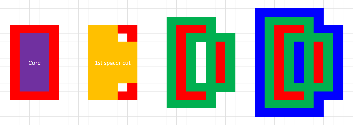
Figure 2. Top views for the SAQP flow of Figure 1, up to the outer gap fill after the 2nd stage spacer. Red: 1st-stage spacer. Green: 2nd-stage spacer. Blue: Core and boundary metal.
Two masks have already been used: one for the core pattern, and one for the first-stage spacer cut. With the third mask, the etch block for the outer gap material, the boundary set of metal wires will be defined. Figure 3 demonstrates a couple of possible outcomes.
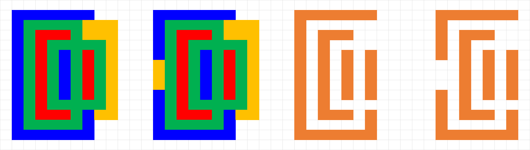
Figure 3. Top views of the completion of the SAQP flow of Figure 1. The yellow areas indicate possible etch block masks which will define the boundary metal features. The orange indicates the final completed metal layouts corresponding to the selected block masks.
Some conditions for this example are that the distance between the two arms of the inner “C” shell metal should be at least 3.5 times metal pitch, and, more importantly, the starting core pattern’s corners should not be terribly rounded. This requires OPC to reduce the corner radius [6], or else possibly using two exposures [7] to sharpen the corners of the starting core pattern if the individual groups of core, shell, and boundary metal lines are too close to one another.
Interestingly, similar patterns to the final results in Figure 3 is revealed in TSMC’s patent US10818779 [8], though for a different purpose (process monitoring).
A generalization of this two-dimensional SAQP approach can be extrapolated to the layouts such as shown in Reference 4 and cited references therein, perhaps providing a path to two-dimensional metal routing at 2nm node.
References
[1] F. Chen, “Feature-Selective Etching in SAQP for Sub-20 nm Patterning.”
[2] F. Chen, “Application-Specific Lithography: 28 nm Pitch Two-Dimensional Routing.”
[3] https://patents.google.com/patent/CN117080054B/zh.
[4] T. Ihara et al., “Grid-based Self-Aligned Quadruple Patterning aware two dimensional routing pattern,” DATE 2016.
[5] F. Chen, “SiCarrier’s SAQP-Class Patterning Technique: A Potential Domestic Solution for China’s 5nm and Beyond.”
[6] Z. Ren et al., “Investigation of the corner rounding effect near the diffraction limit in advanced projection lithography with a rigorous imaging model,” Optics Express 33, 1517 (2025).
[7] C. Sharma et al., “Double exposure double etch for dense SRAM: a designer’s dream,” Proc. SPIE 6924, 692429 (2008).