
SiCarrier's SAQP-Class Patterning Technique: a Potential Domestic Solution for China's 5nm and Beyond

Shenzhen SiCarrier Technologies Co. Ltd. (深圳市新凯来技术有限公司) is a Chinese semiconductor equipment company headquartered in Shenzhen, China, which works closely with Huawei and is backed by the Shenzhen Municipal government [1]. Among 140 Chinese tool firms added to a U.S. commerce trade blacklist last December, the SMIC supplier recently made headlines by claiming its equipment could help China get to 5nm [2]. While the message was obviously promotional, SiCarrier did previously publish a technique to get to 5nm using only DUV lithography [3]. In this article, we’ll take a closer look at what this could entail.
The method disclosed in CN117080054A is often described in the media as “self-aligned quadruple patterning,” but it is not exactly the classical self-aligned quadruple patterning (SAQP) [4] that involves second spacers directly deposited on lines defined by a set of first spacers and etched back. The basic process flow is shown in Figure 1.

Figure 1. Basic process flow disclosed in patent CN117080054A.
It starts off the same as classical SAQP, with first spacers defined on a core pattern. However, then these first spacers are immediately patterned with the cut locations (Figure 2).
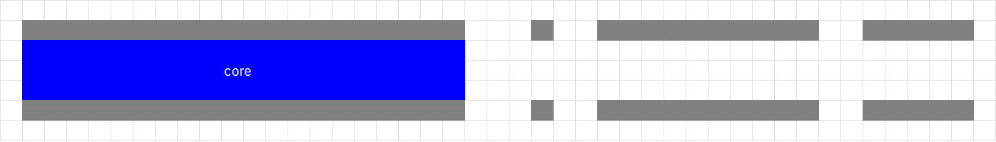
Figure 2. Top view of 1st steps of CN117080054A: (left) 1st spacers deposited and etched back on core pattern; (right) 2nd mask used to define cut locations in the first spacer after core removal.
After the first spacers are cut, then the second spacers are deposited. The trenches in the second spacer film are then filled by a gap-fill material (Figure 3).
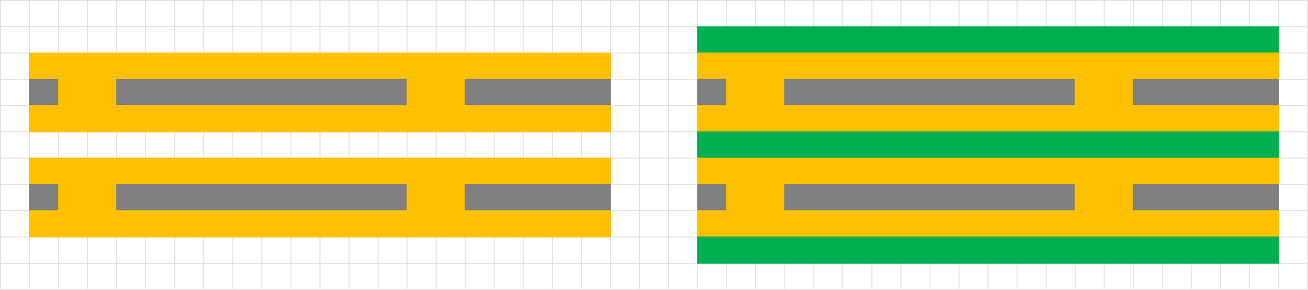
Figure 3. Top view of 2nd spacer steps of CN117080054A: (left) 2nd spacers deposited on cut 1st spacer pattern; (right) trenches in 2nd spacer filled by gap-fill.
A third mask is used to define etch block locations in the gap-fill material (Figure 4).
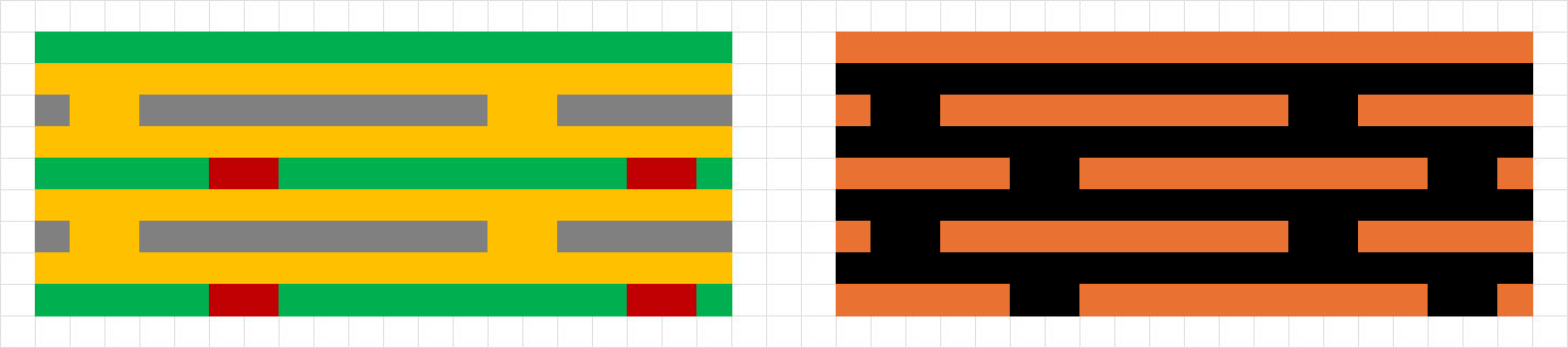
Figure 4. Top view of completion steps of CN117080054A: (left) etch block location defined by 3rd mask in gap-fill material; (right) final pattern after all etching completed.
When the via or cut/block locations are defined by intersecting points of diagonal grid lines [5], the mask count is only three, not overwhelming. For example, this is the case for a horizontal metal track pitch of 28 nm, and a vertical metal crossing pitch of 56 nm (matching an expected track and gate/M1 pitch respectively for 5nm node). In figures 2-4, the cut and block patterns would be mapped to segments of multiple gate/M1 pitch vertical lines. The next connecting metal layer would be defined by 56 nm pitch vertical lines only requiring two cut masks to fit the same diagonal grid (Figure 5).
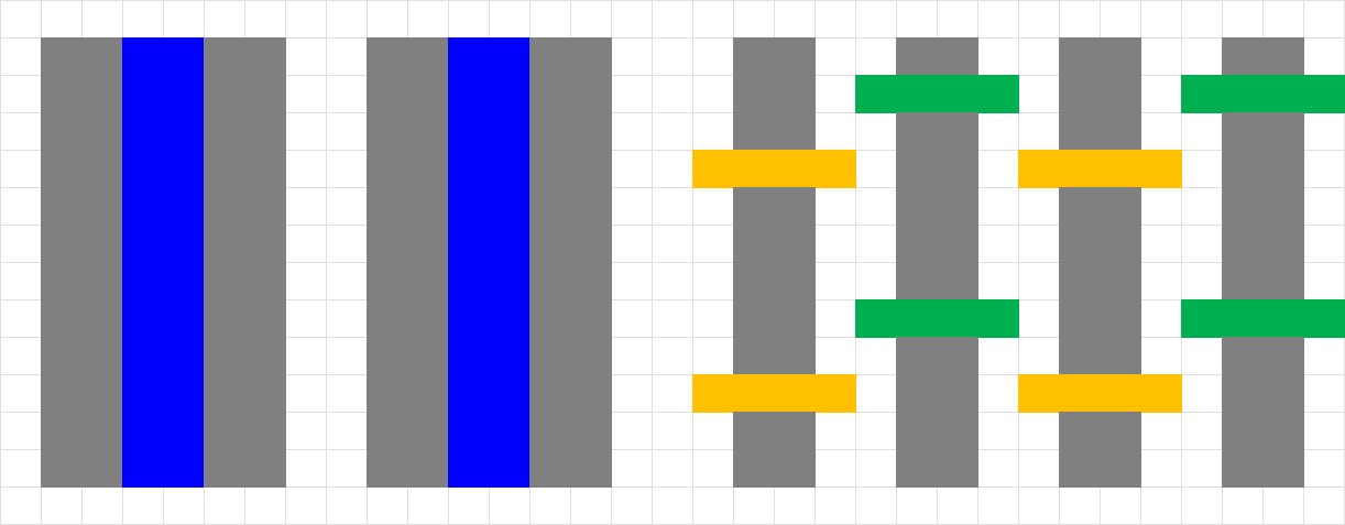
Figure 5. Top view for self-aligned double patterning (left) of metal layer connecting to the one patterned in Figures 2-4. To fit the same diagonal grid, two cut masks (right) are sufficient.
While the example above was based on a fixed pitch metal layer, the patent does describe cases where the spacing between lines or the linewidths themselves may vary. In such cases, to keep the number of masks used to 3 (core plus 1st spacer cut plus 2nd spacer gap block, or core plus 2 spacer cuts), design restrictions would need to be in place to make sure the line break locations are not spaced too close. Since 28 nm pitch is also challenging without EUV multipatterning [6], an approach using three DUV masks would be advantageous against EUV SALELE with cut [7].
References
[1] https://en.wikipedia.org/wiki/SiCarrier
[3] https://patents.google.com/patent/CN117080054A
[4] https://patents.google.com/patent/US5328810A
[5] https://chentfred.substack.com/p/exploring-grid-assisted-multipatterning
[6] P. Leray et al., Proc. SPIE 13424, 1342403 (2025).
[7] R. Venkatesan et al., Proc. SPIE 12292, 1229202 (2022).
Is this only in theory stage or it is ready to commertialise?
Thank you for this excellent post.....