
Exploring Grid-Assisted Multipatterning Scenarios for 10A-14A Nodes

According to the International Roadmap for Devices and Systems 2022 Edition [1], the 10A and 14A logic nodes are expected to have 40 nm gate pitch and 16 nm minimum metal pitch. The latter pitch is often expected to be addressed with 0.55 NA EUV lithography, but in fact a 2 nm electron blur reduces 16 nm pitch image contrast by at least 38%, and more likely it will be close to 58% due to the fast (~80 eV) photoelectrons that do not cluster near where they originate [2]. Thus, we need to consider multipatterning implementations for the 1XA nodes.
A number of aggressive multipatterning scenarios were proposed before [3-7], but now we will focus on fulfilling the following objectives:
minimizing the number of masks used for the 14A and 10A nodes.
ensuring straight cuts of metal lines, entailing the use of a cut line grid.
leveraging fully self-aligned via patterning.
This leads us to considering the dual etch-selectivity approach shown in [6] (and also used in [3] and [4] and the diagonal grid approach shown in [7].
Dual Etch-Selectivity
The dual etch-selectivity approach conveniently leverages the inherent difference of material between the (final) spacer core and spacer gap in self-aligned double patterning (SADP), self-aligned quadruple patterning (SAQP), or even self-aligned octuple patterning (SAOP). The advantage of this approach is that a block or cut pattern can extend well beyond the metal line to be cut, without affecting the adjacent line (Figure 1).
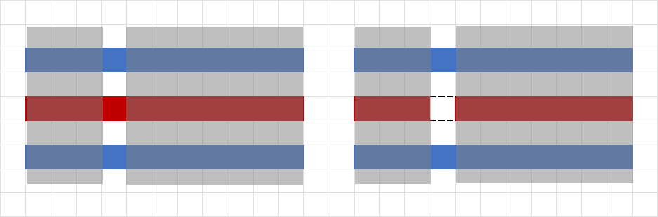
Figure 1. In a dual etch-selectivity scenario, the red track can be etched where exposed, without the adjacent blue tracks being affected, at least ideally.
For a metal track layer, we can expect the following mask steps (see Figure 2):
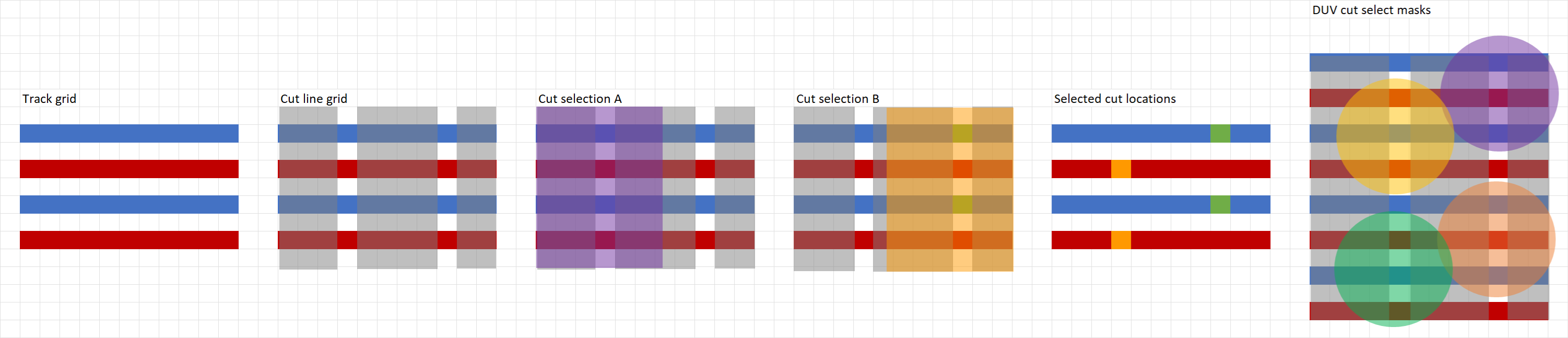
Figure 2. Grid-assisted multipatterning using dual etch-selectivity.
Metal track grid - 1 EUV mask/SAQP or 1 DUV mask/SAQP or SASP or SAOP as needed. The final spacer separates tracks of two different materials to be etched.
Cut line grid - 1 DUV or EUV mask/SADP
Cut selection - One EUV mask or two DUV masks (minimum pitch or center-to-center ~ 100 nm), per track material to be etched.
Note that the metal track grid is taken to have a pitch equal to the minimum metal pitch of 16 nm, while the cut line grid is taken to have a pitch equal to the gate pitch of 40 nm.
An EUV-free implementation would require 6 DUV masks, whereas an EUV user may choose to use 2 EUV masks for cut selection, and 2 DUV masks for the grids.
For cut selection, an EUV mask could be replaced by two DUV masks. In comparing one EUV exposure vs. two DUV exposures, cost [8-10], availability [11], and throughput still favor the latter [12].
The key disadvantage of dual etch-selectivity approach is that it doubles the number of masks for removing portions of lines, as each mask only works for etching half of the lines. Consequently, for the cut selection, four DUV mask exposures or two EUV mask exposures are required for dual etch, whereas for a conventional single etch only two DUV mask exposures or a single mask exposure would be required.
For via layer patterning [7], the required mask number is the same as cut selection: four DUV mask exposures or two EUV mask exposures. This is because the via etch and trench etch must match material to be etched. The full process integration can be quite complicated [4].
Diagonal Grid
Diagonal grids have been proposed for via placement for better manufacturability [13,14]. A diagonal via grid naturally maps two adjacent metal lines at different voltages on one layer to two adjacent metal lines on an underlying layer (Figure 3). A diagonal cut grid naturally fits the diagonal via grid, as line breaks naturally fall next to via landings.
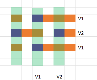
Figure 3. A diagonal via (blue) grid naturally maps two adjacent metal lines at different voltages on one layer to two adjacent metal lines on an underlying layer.
The diagonal grid approach adds a diagonal line grid to first extract the cut locations from the cut line grid (Figure 4). This allows a single trench etch to be used for the tracks.
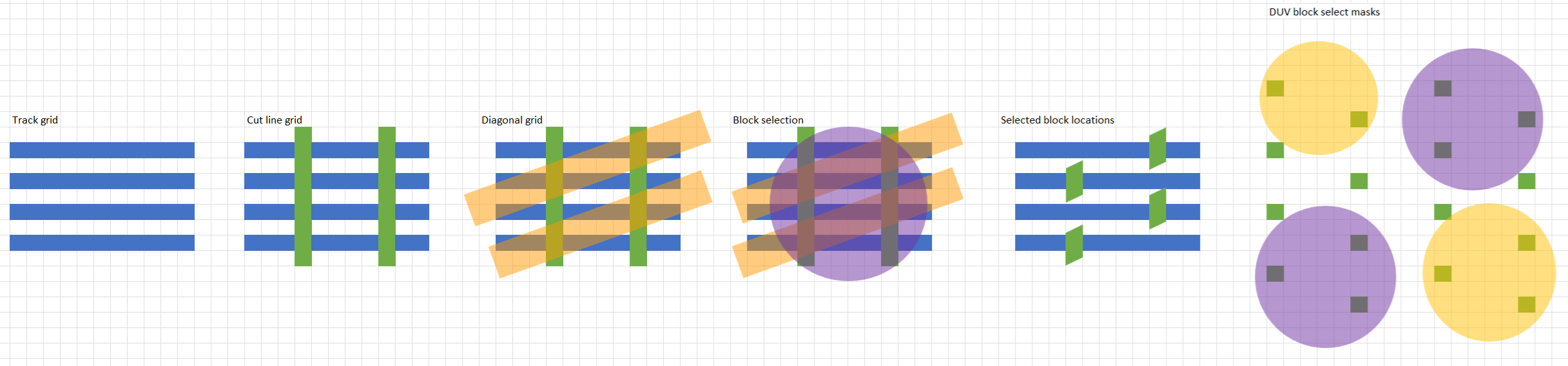
Figure 4. Grid-assisted multipatterning using diagonal grid.
For a metal track layer, we can expect the following mask steps:
Metal track grid - 1 EUV mask/SAQP or 1 DUV mask/SAQP or SASP as needed
Cut line grid - 1 DUV or EUV mask/SADP
Diagonal grid - 1 EUV mask/SADP or 1 DUV mask/SATP or SAQP
Block selection - One EUV mask or two DUV masks (minimum pitch or center-to-center ~ 100 nm).
As shown in Figure 4, the diagonal lines in the diagonal grid cross one metal track as they cross one gate pitch, and are spaced so that adjacent diagonal lines intercept cut locations or vias two metal tracks apart.
Here, an EUV-free implementation would require 5 DUV masks, whereas an EUV user may choose to use 1 EUV mask for cut selection, and 3 DUV masks for the grids. Again, using the 2 extra DUV masks is preferable to the single EUV mask, due to cost, throughput, and availability.
Moreover, in the future SAQP, SASP, and SAOP may use new techniques such as directed self-assembly [15] or atomic-layer-etching pitch splitting [16], further simplifying the process flow for grid patterning.
With the diagonal grid approach, for fully-self-aligned via layer patterning [7], the required mask number is less than for dual etch-selectivity: three DUV mask exposures or two EUV mask exposures.
Diagonal grid - 1 EUV mask/SADP or 1 DUV mask/SATP or SAQP
Via selection - One EUV mask or two DUV masks (minimum pitch or center-to-center ~ 100 nm).
While the diagonal grid mask is added, the number of cut selection masks is halved, resulting in a net reduction of masks.
Summary
Tables 1 and 2 show the summary comparison of the multipatterning approaches for metal track and fully-self-aligned via layers, respectively.
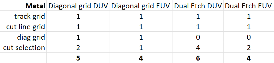
Table 1. Metal track layer gridded multipatterning approaches comparison.
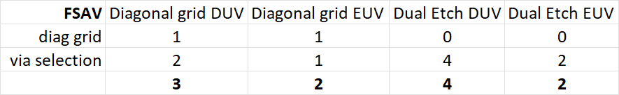
Table 2. Fully-self-aligned via layer gridded multipatterning approaches comparison.
In short, the inevitable use of greater degrees of multipatterning does not need to entail an explosion of mask use. However, it would lead to more complex etch process development or a restriction in feature placement and routing.
References
[1] https://irds.ieee.org/editions/2022/irds%E2%84%A2-2022-lithography
[2] F. Chen, A Realistic Electron Blur Function Shape for EUV Resist Modeling; Revisiting the Electron Blur Function Shape in EUV Lithography
[3] F. Chen, Extension of DUV Multipatterning Toward 3nm.
[4] F. Chen, BEOL Mask Reduction Using Spacer-Defined Vias and Cuts.
[5] F. Chen, Self-Aligned Block Redistribution and Expansion for Improving Multipatterning Productivity.
[6] WIPO Patent Application WO2016134954, assigned to ASML.
[7] F. Chen, Multipatterning Reduction with Gridded Cuts and Vias.
[8] E. Vidal-Russell, J. Micro/Nanopattern. Mater. Metrol. 23, 041504 (2024).
[9] L-A. Ragnarsson et al., EDTM 2022.
[10] J. van Schoot et al., 2021 EUV-FEL Workshop.
[11] C-H. Chang, M-W. Chen, A-J. Ma, C-Y. Chen, US Patent Application 20220382168.
[12] ASML 2023 annual report, p. 87.
[13] P. Woltgens et al., Proc. SPIE 12051, 120510I (2022).
[14] S-W. Peng, C-M. Hsiao, C-H. Chang, J-T. Tzeng, US Patent Application 20230387002.
[15] S. Xiong et al., ACS Nano 10, 7855 (2016).
[16] J. Sundqvist et al., SPIE Advanced Lithography & Patterning 2025, Paper 13429-28, Atomic layer etching pitch splitting (APS): a new alternative to self-aligned double patterning | SPIE Advanced Lithography + Patterning
Thank you for sharing this insight into enhancement of advanced lithography.....
Video to accompany this article: https://www.youtube.com/watch?v=Yc3yKZGXIx4