
Crossed Self-Aligned Multipatterning For Sub-40 nm Pitch Grids: A Process On Record For DRAM

Certain patterns such as hexagonal hole or pillar arrays [1] or metal cut grids [2,3] lend themselves naturally to crossed self-aligned multipatterning (X-SAMP). For the D1b or 12nm-class generation of DRAM, for example, we expect storage nodes to be separated by less than 40 nm. However, EUV suffers from substantial stochastic effects affecting storage node shape and positioning [4]. State-of-the-art DRAM uses X-SAMP to create the hole patterns for the capacitor array [5].
The process flow for crossed self-aligned double and quadruple patterning has already been disclosed publicly [6]. The steps for the case of X-SAQP are shown below (Figure 1) [1]. The key requirement is for the materials involved to be able to be etched selectively with respect to the others. These materials are typically selected from silicon oxide, silicon nitride, carbon, silicon, metal (e.g., TiN), and even metal oxide (e.g., Al2O3).
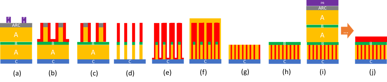
Figure 1: Steps for X-SAQP, based on Ref. [1]. (a) Deposition of process stack and 1st mandrel lithography. (b) Mandrel formation and spacer deposition. (c) Spacer etch-back. (d) Etch of underlayers to extend mandrel vertically. (e) 2nd spacer deposition. (f) Filling gaps between 2nd spacers. (g) Planarization by etch-back. (h) Coat for cross-layer patterning. (i) Deposition of 2nd process stack and 2nd mandrel lithography. (j) Repeat steps (a) through (g) in 2nd process stack.
The formation of holes or pillars depends on the followup etch sequence after the two patterned process stacks are prepared. Figures 2 and 3 show the sequences for where the intersection of the lower and upper spacers define the final grid holes and pillars, respectively. An obvious modification could alternatively use the intersection of gaps between spacers.
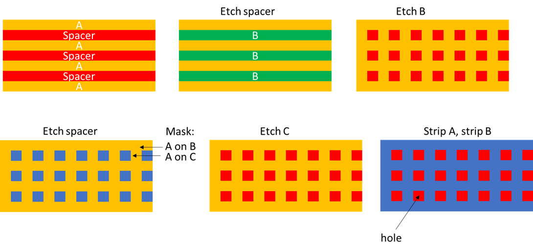
Figure 2. Etch sequence for an array of holes (top view).
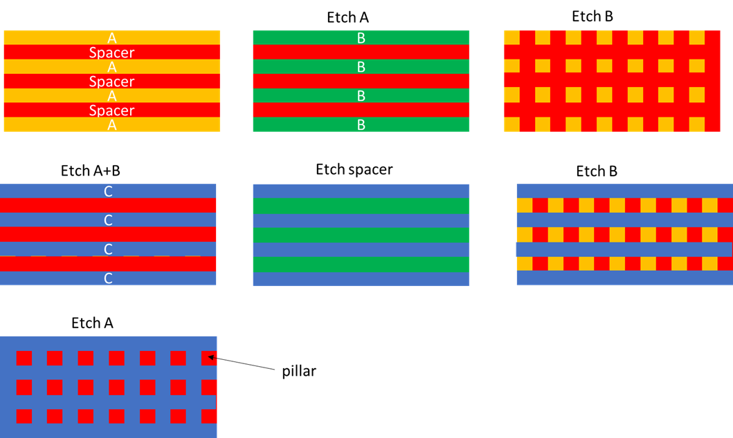
Figure 3. Etch sequence for an array of pillars (top view).
It is apparent that the X-SAMP approach is more etch-intensive than litho-intensive, although it is still necessary to align the 2nd mandrel lithography with the 1st. Nevertheless, in a published demo [1], the X-SAQP approach achieved better patterning performance than EUV (Figure 4).
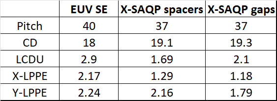
Figure 4. EUV vs. X-SAQP patterning comparison for hexagonal hole arrays[1].
Significantly higher EUV doses would lead to unwanted throughput loss [7] as well as resist loss [8]. There are other possible alternatives to X-SAMP which are cheaper than EUV, including directed self-assembly (DSA) [5] and nanoimprint [9], but for now, X-SAQP does have the weight of being a process on record (POR).
References
[1] N. Bae et al., Proc. SPIE 11615, 116150B (2021).
[2] F. Chen, Exploring Grid-Assisted Multipatterning Scenarios for 10A-14A Nodes; F. Chen, Multipatterning Reduction with Gridded Cuts and Vias.
[3] M. C. Smayling et al., Proc. SPIE 8683, 868305 (2013).
[4] F. Chen, Aggravated EUV Stochastics With Hexapole Illumination.
[5] Md. S. Rahman et al., Proc. SPIE 13427, 134270G (2025).
[6] Q. P. Wang, Pathfinding by process window modeling: Advanced DRAM capacitor patterning process window evaluation using virtual fabrication.
[7] J. Lee et al., Proc. SPIE 12495, 124950S (2023).
[8] F. Chen, Resist Loss Model for the EUV Stochastic Defectivity Cliffs; F. Chen, Resist Loss Prohibits Elevated EUV Doses.
[9] M. Ogusu et al., Proc. SPIE 12497. 1249709 (2023).