
Sub-10 nm Half-Pitch Density Multiplication by Directed Self-Assembly

Pitch Shrinking Requires Multipatterning
Multipatterning has been the go-to method for sub-20 nm half-pitch features, even when used with the highest resolution techniques such as electron-beam lithography [1,2] and EUV lithography [3,4]. This situation has come about since stochastic effects plague the formation of patterns in the highest resolution resists due to photon shot noise as well as electron scattering [5,6]. Whether using multiple exposures or multiple spacer deposition and etch steps, traditional multipatterning techniques for reducing pitch have been a source of increased complexity and cost for advanced process nodes. Enter directed self-assembly.
Directed Self-Assembly: A Timely Alternative for Sub-20 nm Pitch
Directed self-assembly (DSA) was disclosed over a decade ago as a way of achieving sub-10 nm half-pitch [7]. DSA uses a unique property of block copolymers (BCPs) to produce repeated nanopatterns. Block copolymers spontaneously separate into different phases when the two ends of one molecule are sufficiently different in chemical characteristics; the size of the phases is dependent on the molecular weight of each end [7]. BCPs form microphase-separated structures with periodic lengths ranging from a few to tens of nanometers, depending on key parameters such as the degree of polymerization (N), volume fraction (f), and Flory–Huggins interaction parameter (𝜒), of the polymers [8]. The parameter 𝜒 represents how well the two components mix together; 𝜒>0.5 means that phase separation will occur due to poor mixing.
Earlier this year, Science Tokyo, IMEC, and TOK published a paper which demonstrated 5x density multiplication using polystyrene-block-[poly(glycidylmethacrylate)-random-poly(methyl methacrylate)], functionalized with 2,2,2-trifluoroethenethiol (PS-b-PS-b-PGFM) [8]. The process flow is shown in Figure 1. This process enabled the use of 90 nm pitch guide lines patterned by ArF immersion lithography to support the formation of BCP phase separation images with 1/5 the pitch, i.e., 18 nm. DSA was completed in an acceptable 5 minutes annealing time.
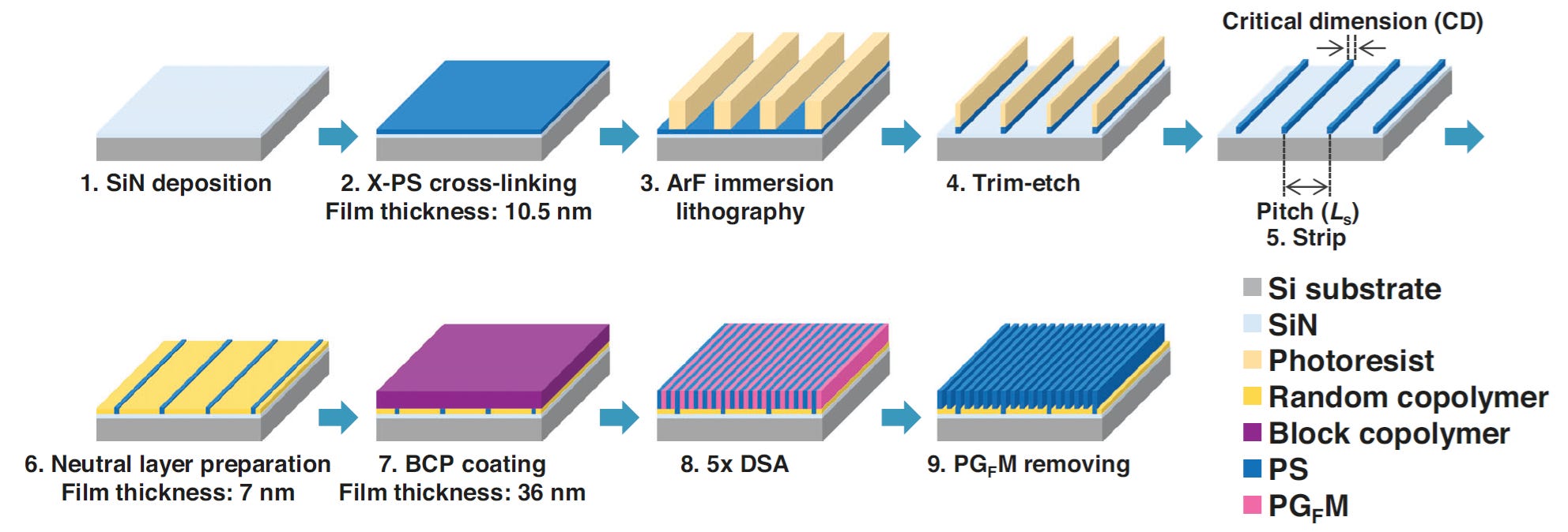
Figure 1. Process flow for 5x density multiplication by DSA using PS-b-PS-b-PGFM. 90 nm pitch chemical guide lines support the DSA pitch of 18 nm. From ref. [8].
Addressing Defectivity
As with any new patterning technology, defectivity needs to be addressed. Two types of defects were identified: (1) parallel areas, where the phases were oriented parallel to the surface instead of perpendicular, and (2) dislocations. Line patterns without parallel-oriented structures or dislocations can be achieved by optimizing the chemical guide CD and annealing temperature. Decreasing the BCP thickness is also expected to help reduce the defect risk. Furthermore, line roughness is improved by increasing chemical guide pitch and/or 𝜒N.
Can DSA be a Patterning Panacea?
While sub-10 nm half-pitch lines are demonstrated here, can DSA be similarly applied to other patterning cases like blocks/cuts and vias? In fact, such applications have been discussed or demonstrated more than once before. Fixed pitch patterns appear easier to optimize with chemical guiding patterns (chemoepitaxy [8]) [11]. On the other hand, more free-form patterns have relied on topography guiding patterns (graphoepitaxy [8]) [9,10], and therefore face more constraints in optimization. Undoubtedly, work will continue in this promising field, as the motivation to reduce process complexity and equipment costs while maintaining acceptable throughput is very strong.
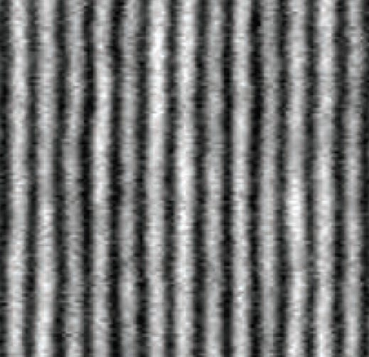
Figure 2. 9 nm half-pitch by the DSA process shown in Figure 1.
References
[1] W. Chao et al., “Double patterning HSQ processes of zone plates for 10 nm diffraction limited performance,“ International Symposium on Electron, Ion, and Photon Beams and Nanolithography, 2009.
[2] T. Kono et al., “Half-pitch 14nm direct patterning with nanoimprint lithography,” Proc. SPIE 10958, 109580H (2019).
[3] A. Raley et al. “Outlook for high-NA EUV patterning: a holistic patterning approach to address upcoming challenges,” Proc. SPIE 12056, 120560A (2022).
[4] P. Leray et al., “NA0.33 EUV extension for HVM: testing single patterning limits,” Proc. SPIE 13424, 1342403 (2025).
[5] F. Chen, Facing the Quantum Nature of EUV Lithography.
[6] M. Kotera et al., “Dependence of linewidth and its edge roughness on electron beam exposure dose,” J. Vac. Sci. Tech. B 23, 2775 (2005).
[7] M. Watts, Directed Self Assembly – record breaking small features.
[8] S. Maekawa et al., “High-Fidelity Directed Self-Assembly Using Higher-χ Polystyrene-Block-Poly(Methyl Methacrylate) Derivatives for Dislocation-Free Sub-10 nm Features,” Adv. Func. Mat. 35, 2421066 (2025).
[9] Z. Wu et al., “Quadruple-hole multiplication by directed self-assembly of block copolymer,” Proc. SPIE 13423, 134231O (2024); F. Chen, China’s Multipatterning Breakthrough? Quadruple Hole Patterning by Directed Self-Assembly on a Staggered Via Grid.
[10] Z. Xiao et al., “DSA Template Mask Determination and Cut Redistribution for Advanced 1D Gridded Design,” Proc. SPIE 8880, 888017 (2013).
[11] Md. S. Rahman et al., “Directed Self-Assembly of Medium-Chi and High-Chi Block Copolymers for DRAM C/H Patterning,” Proc. SPIE 13427, 134270G (2025).