
SMIC's SAQP + LELE Patterning Approach: Choosing Flexibility over Density
Minimum pitch in the same class as 3nm/2nm nodes, but emphasis on design flexibility will sacrifice transistor density despite comparable standard cell heights

Just a few days ago, I came across a very interesting patent application filed by SMIC, filed in both China [1] and the US [2]. Probably the first aspect that drew my attention was how recent it was. It was first filed in China in October 2024. The goal was to increase design flexibility while increasing device density. While self-aligned quadruple pattering (SAQP) is effective for achieving pitches less than 30 nm, thereby increasing density, it leads to restrictions on design layouts. For example, SAQP naturally leads to pairs of feature pairs. On the other hand, features that can be patterned by a more conventional double patterning approach such as LELE (Lithography+Etch, doubled) have more flexibility in feature size and spacing. SMIC proposes to accommodate both density and flexibility targets by having some zones on the chip which are patterned by SAQP and other zones which are patterned by LELE.
The SAQP Zone
In the patent applications, SMIC says it is targeting a minimum pitch of 24 nm. In fact, SAQP with an immersion machine operating at 193 nm wavelength and 1.35 NA allows even going down to 19 nm. As the number of masks used for SAQP should be minimized as much as possible and the processing also not too complex, the standard cell should have an odd number of signal tracks between the Vdd and Vss rails, without constraining the rail widths [3]. For example, with 5 signal tracks between double-width rails, the cell height becomes 6.5 track metal pitches (Figure 1). For a track metal pitch of 24 nm, this becomes 156 nm. This cell height is within the range of cell heights used for TSMC’s 3nm [4] and 2nm [5] nodes.
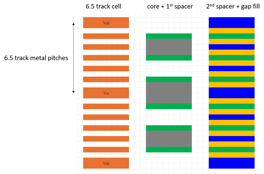
Figure 1. 6.5-track cell formed by SAQP. Left: track layout. Center: Core pattern (gray) with first spacer (green). Right: Second spacer (yellow) with gap fill (blue).
One mask would be needed to produce the 5 signal lines between rails at these pitches. This mask would define the starting core, or mandrel, pattern. To complete the layout in the SAQP zone, up to 4 more masks would be needed (Figure 2). Now that there is also an LELE zone, we might expect 2 additional masks to be needed, but that is exactly what SMIC’s patent application is able to avoid.
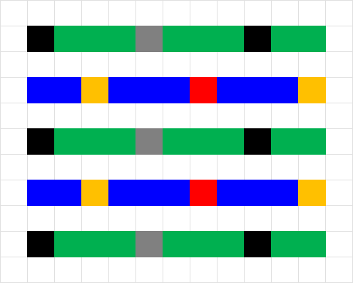
Figure 2. Green: lines defined by 1st spacer. Blue: lines defined by gaps between 2nd spacer. Black, gray, yellow, red locations each indicate a self-aligned cut or block site from a given mask. Due to the layers deposited during the process flow, the blue and green lines can be cut/blocked separately, not simultaneously.
The LELE Zone
After the first mask patterns the SAQP core features, a first spacer is deposited over those features and etched back. These eventually will be used to form a hardmask pattern in the SAQP zone. Outside, in the LELE zone, the hardmask layer is patterned by LELE (two masks) to pattern the looser pitch features; the patent application specifies it can be as low as 38 nm. The specific embodiment shown is the really interesting part; instead of forming a second trench pattern (3rd mask, Figure 4) after a first trench pattern (2nd mask, Figure 3), the second trench pattern actually has the tone reversed. The third mask is also used to open up some areas in the SAQP zone, which are targeted to be rendered effectively unetchable by ion implantation. This constitutes the 1st “block mask” in the SAQP zone. By combining two functions into the same mask, overall mask count can be reduced. Note that the features which are blocked from being etched are portions of the 1st spacer pattern. The remaining masks are to cut parts of the 1st spacer pattern as well as areas of the LELE zone (Figure 5), and subsequently, to add blocking areas to portions of the gaps between the second spacers in the SAQP zone as well as areas of the LELE zone (Figure 6).
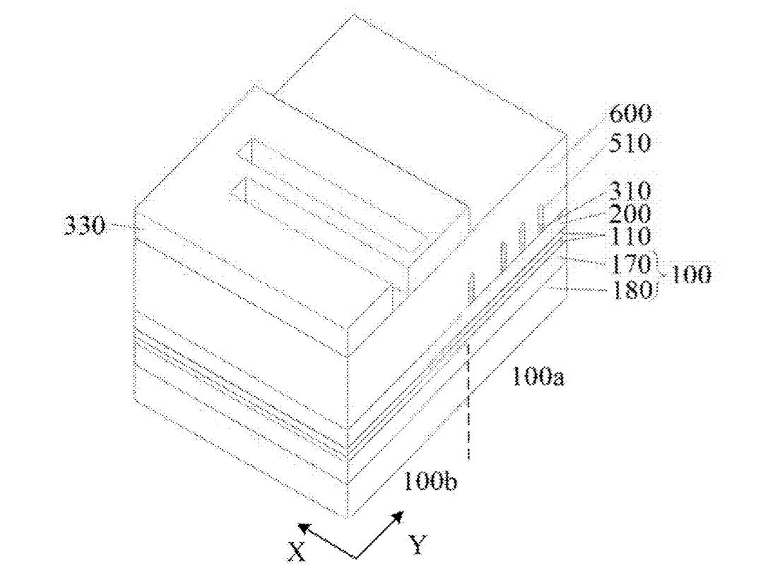
Figure 3. 2nd mask defines first trench in the LELE zone [2].
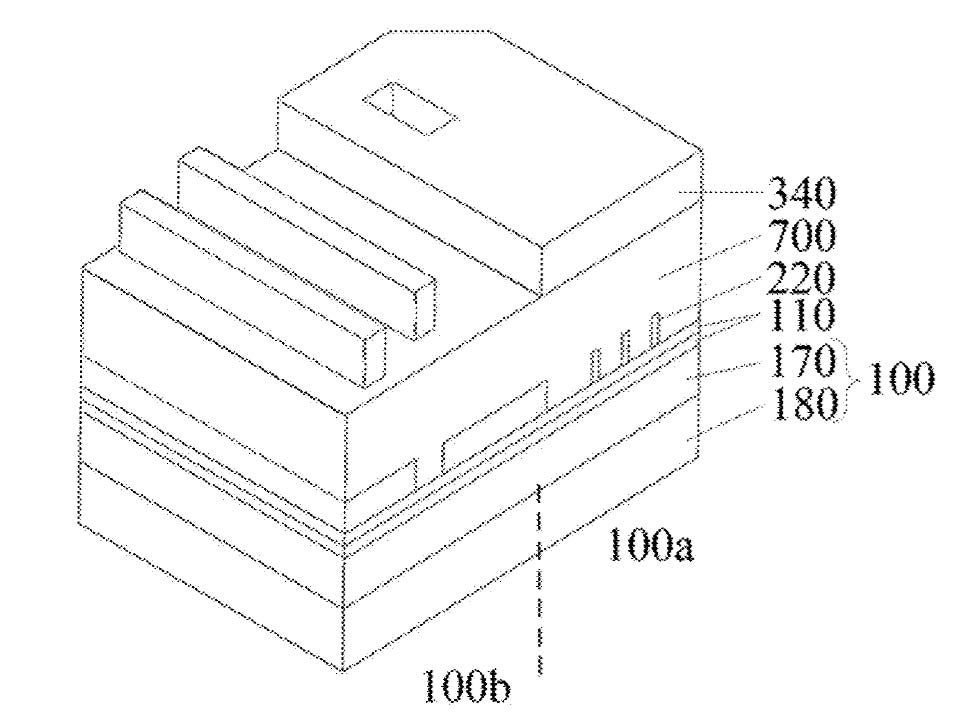
Figure 4. 3rd mask defines second trench in the LELE zone and first area to be blocked in the SAQP zone, affecting 1st spacer patterns only [2].
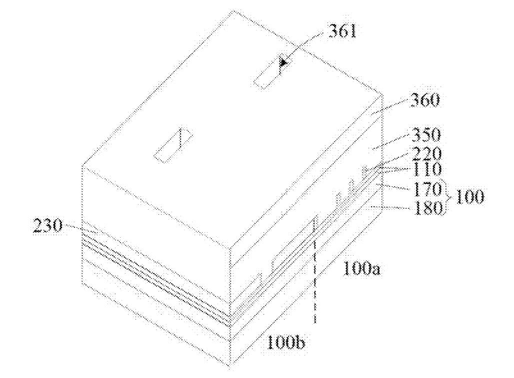
Figure 5. 4th mask cuts parts of the 1st spacer pattern in the SAQP zone as well as areas of the LELE zone [2].
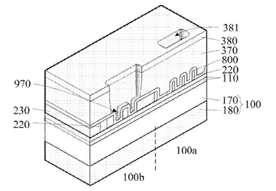
Figure 6. 5th mask blocks areas of portions of the gaps between the second spacers in the SAQP zone as well as areas of the LELE zone [2].
In fact, the whole process sequence can be made even simpler, i.e., avoiding tone reversal and ion implantation. The 2nd and 3rd masks could be simultaneous LELE in the LELE zone and 1st spacer cuts in the SAQP zone. Then the last two masks (4th and 5th) could be blocking areas for the LELE zone as well as for portions of the gaps between the second spacers in the SAQP zone. But this flow is a bit too mundane and would not be suitable for a patent application.
If we skipped the LELE zone and just had the SAQP zone, we would still need up to five masks (core masks plus the four cut/block masks). So, adding the LELE function does not incur any mask cost. There is some extra process complexity for sure, to accommodate the added diversity of the patterns.
In short, the objective of SMIC’s patent application appears to be focusing on adding design flexibility with looser pitches rather than enhancing transistor density. This may also be consistent with Huawei’s recent tau scaling emphasis, since steadfastly shrinking pitch goes against this path [6].
References
[1] CN121925109A, assigned to SMIC.
[2] US20260114246, assigned to SMIC.
[3] J. U. Lee et al., Proc. SPIE 10962, 109620N (2019); US10418244, assigned to Qualcomm; F. Chen, Kirin 9030 Hints at SMIC’s Possible Paths Toward >300 MTr/mm2 Without EUV.
[4] 3 nanometers, what to do? - Electronic Headlines - EEWORLD Electronic Engineering World.
[5] TSMC N2P Process Preview · Kurnal Insights.
[6] F. Chen, Huawei’s Logic Folding: How it Could Simplify Multipatterning.
Thank you for sharing this article with us. We had few challenges with Overlay varians and contribution to CD, Defects and yield at 5nm node...