
A Subtle Design Rule Implementation Can Significantly Reduce Multipatterning
Another benefit for tip-to-tip relaxation

Design rules play an important role in maintaining the manufacturability of a given layer in a chip. Via enclosure and minimum metal spacing are examples of design rules which need to be tightly controlled in order to preserve electrical connections signal integrity. Some design rules are important also for process yield. An example that demonstrates this in more than one way is the tip-to-tip (T2T) distance between line ends. Besides potential arcing or dielectric breakdown between the line ends, the patterning manufacturability is also at stake. The smaller T2T fundamentally leads to worse depth of focus [1]. This turns out to be a serious problem for High-NA EUV lithography [2]. More subtly, though, relaxing T2T can be beneficial for multipatterning, as will be explained below.
Self-Aligned Vias
In the fully self-aligned via (FSAV) process [3], the via is defined by the edges of both upper and lower metals. This allows vias to be patterned with larger size in both x and y directions, resulting in larger metal contacting area and, at the same time, less sensitivity to overlay in both x and y. However, T2T indirectly affects the number of masks needed to pattern a FSAV layout.
In Figure 1, the T2T is taken to be equal to the metal half-pitch. It is seen that any exposure area that includes the diagonal via pair will also spills onto areas where the upper and lower metals intersect but are not supposed to form vias.
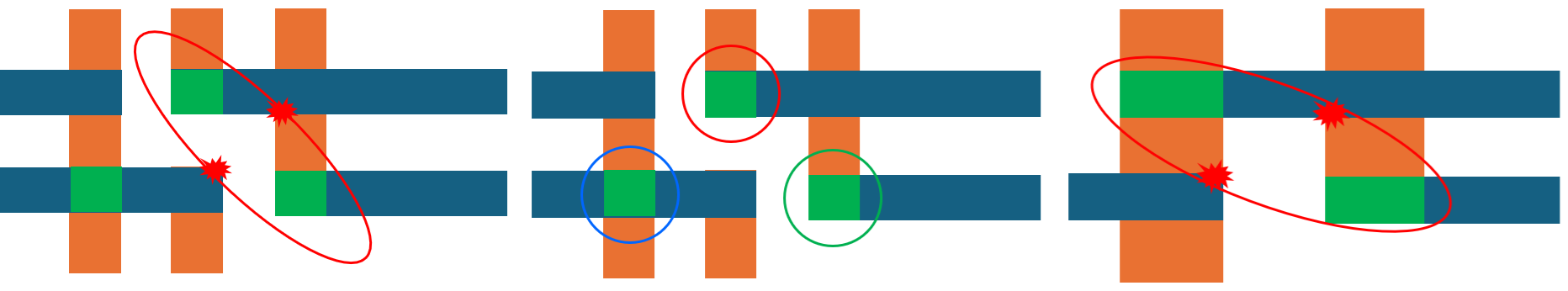
Figure 1. (Left) When the T2T equals the half-pitch, the pair of diagonal vias cannot be patterned together since the exposure area that includes them will also expose parts of FSAV locations which are not supposed to have vias. (Center) The vias shown must therefore be patterned individually, requiring (at least) three different mask exposures. (Right) Even if one of the metal pitches is expanded, if the T2T matches the expanded half-pitch, the same issue still comes up.
If instead, we establish the rule that the T2T must exceed the metal pitch, the situation changes dramatically (Figure 2).
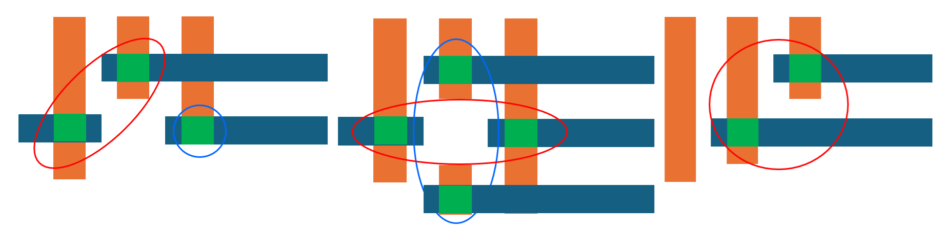
Figure 2. When the T2T is required to be at least the metal pitch, two exposures are sufficient to expose the three vias.
Now, with one less corner intersection of lower and upper metal layers in the vicinity, it is easy to use at most two exposures instead of three (or more) to pattern the three vias. Expanding to larger layouts, it can be shown that LELE (2x litho+etch) double patterning with ArF immersion lithography can handle realistic 3nm-level layouts (Figure 3) [4,5].
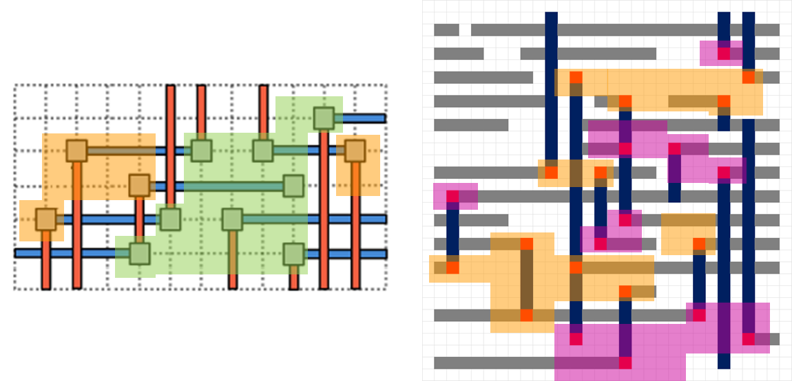
Figure 3. LELE double patterning for self-aligned via layouts where the T2T is sufficiently large. Each colored region is assigned to a designated mask. Sources: [4] (left), [5] (right). A 12 nm metal half-pitch is assumed here.
Metal Line Cuts
A relaxed T2T distance could also help reduce the number of cut masks. Larger T2T distances create opportunities to merge cuts on different lines. However, even with larger T2T allowed, shorter metal lines tend to prevent a substantial reduction in the number of masks, since they naturally reduce the cut pitch.
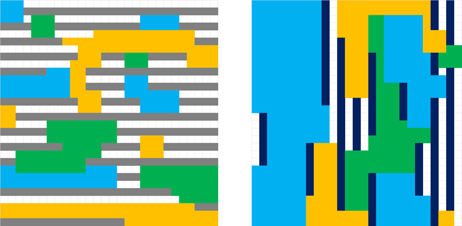
Figure 4. Cut masks (each a different color) assigned to the metal layers for the layout on the right in Figure 3.
Taking the layout on the right in Figure 3 as an example, it is unavoidable to use three masks, assuming the 24 nm metal pitch and ~100 nm minimum feature separation for 193 nm immersion lithography. However, if we had a T2T of only a metal half-pitch, cut merging across lines would not be possible, and we would easily exceed four masks.
Thus, relaxed T2T greatly reduces the DUV multipatterning burden. This should be welcome relief to foundries without EUV. Even for EUV users, though, this can hopefully ease the dependence on ASML’s EUV systems as well as the necessary EUV multipatterning.
References
[1] F. Chen, Tip-to-Tip Limitations on Depth-of-Focus: When Higher NA Does Not Help.
[2] W. Gao, C-K. Chen, J. Zimmermann, “Computational evaluation of critical logical metal layers of pitch 20-24nm and the aberration sensitivity in high NA EUV single patterning,” Proc. SPIE 12495, 1249509 (2023).
[3] W. Gao et al., ”Simulation investigation of enabling technologies for EUV single exposure of Via patterns in 3nm logic technology,” Proc. SPIE 11323, 113231L (2020).
[4] Y-N. Tsai and S-Y. Fang, “Via Fabrication with Multi-Row Guiding Templates Using Lamellar DSA,” ASPDAC 2025.
[5] Y-T. Lin, K-T. Fan, I. H-R. Jiang, “Multi-Row Guiding Template Design for Lamellar Directed Self-Assembly with Self-Aligned Via Process,” ACM Trans. Des. Autom. Electron. Syst. 30, 2, Article 29 (2025).
TSMC disclosed its work on fully self-aligned vias in 2021: https://ieeexplore.ieee.org/document/9720600, likely too late for its N3 release. Hopefully, it's ready to use now.